Results
The results of the project will be compiled in the order of individual component structure, 1-bit
design, and finally full 8-bit functionality. More specifically, the order will be: mux, xor, full
adder, register, 1-bit, then 8-bit.
MUX
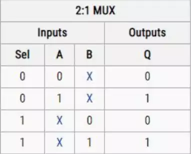
The Mux can be thought of using the following expression: $$Mux21(a,b)= (A\circ\bar{S}_{0})+(B\circ S_{0})$$
Its function is rather simple, and is clearly used as a selector of two inputs. In the design used in
this project, the mux selects between previously computed data from the register and new data in
the form of vector B. In terms of the above equation, "A" is the register data, while "B" is vector
B and its components.
In terms of this picture, "In_1" corresponds to vector B and "In_0" is the register output. Just as
in an inverter, the two sides of the mux use a single n-channel fet and a single p-channel fet. The
selector, or "S0" in the equation, is used to update the output by connecting to both gate clusters.
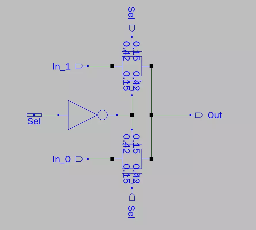
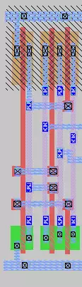
This right figure is the magic layout used for mux operation. It
includes an inverter on the left side to create the "Sel_bar" input
attached to the gates of the n-channel on the register input and the
p-channel on the B vector input. The other four gates on the right
side of the image comprise the remaining logic which is actuated by
Sel and Sel_bar, where the value of either In_0 or In_1 is passed to
the output.
The two below images were compared against the truth table to
verify their functionality. The top-most of the two images is the
IRSIM result of the provided Sue schematic, while the lower image
is of my own VLSI drawing.
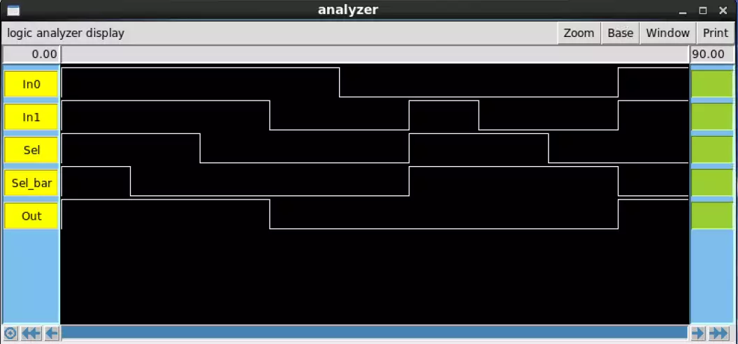
The Sue IRSIM works according to the truth table, however the Sel_bar was set manually rather
than being an inverter form of the select signal. Regardless of this, the output was correct
according to the inputs and equation.
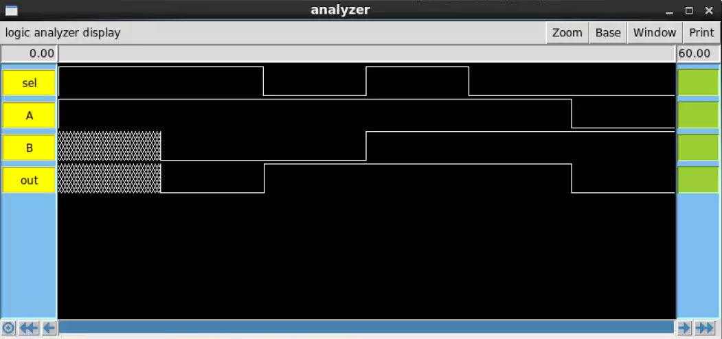
Finally, the magic IRSIM lacks the Sel_bar output as the design includes an inverter that
automatically takes the Sel input and inverts it. Regardless of this, the output still works just as it
should.
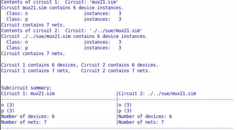
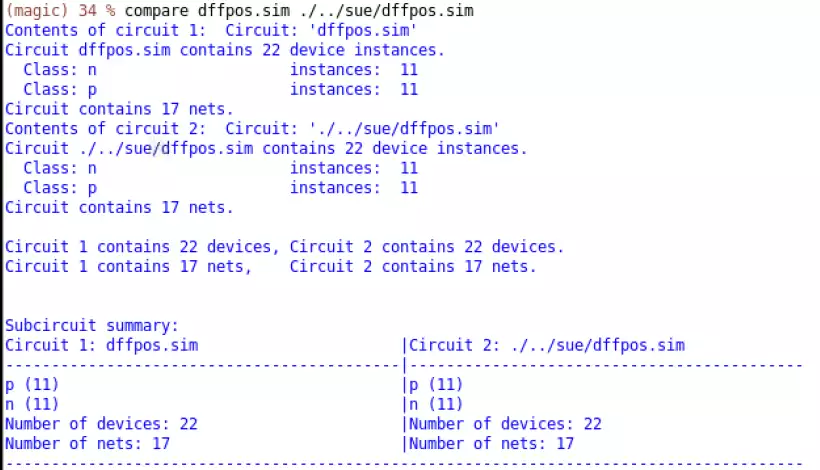
The last verification of the Mux is IRSIM which passed. The number of transistors for both the
sue and magic circuit match, as well as the number of nets.
Xor
An Xor gate stands for exclusive or, meaning that the truth table differs from a standard "or" gate
in that when both inputs are high, the output is low. When the same inputs are given to an "or"
gate, the result is true.
$$Q=A\vee B=A\oplus B=(A\neq B)$$
The above equation is rather simple, but the implementation is slightly harder than that of the
mux. In essence, Q will be high when either A or B is high, but not both.
The center 8 mosfets are akin to a traditional "or" gate, however an inverted form of both "A"
and "B" are added in series to both the n and p sides. The left and right most clusters are the
inverters for the two input signals. In terms of the overall system, the subtraction signal is sent
into the "b" input of the xor gate while the A vector is sent into the "a" input of the xor gate. It
does not matter which input is "a" or "b," as both sides of the circuit are the same and the output
will be identical regardless of configuration.
This picture on the right is the magic
layout used to complete the function of the
exclusive or. It is basically identical to the
sue schematic in terms of layout, as the
two inverters are located on the outside,
and the eight mosfet logic structure is
located centrally.
The two below images were compared
against the truth table to verify their
functionality. The top-most of the two
images is the IRSIM result of the provided Sue schematic, while the lower image is of my own
VLSI drawing.
The Sue IRSIM test is very simple and includes every possibility according to the above truth
table. All outputs are correct with respect to the given inputs.
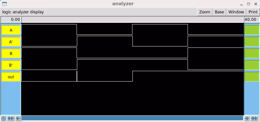
This Magic IRSIM includes the inverted signals of A and B, which are shown to work correctly.
The overall logic of the system is identical to both the Sue IRSIM and truth table.
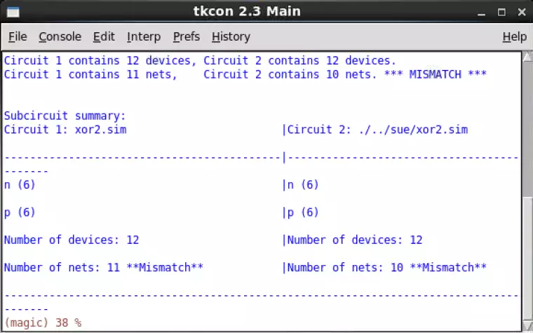
The LVS test of the exclusive or gate passes in terms of gate quantity, but the number of nets
does not match. Both the Sue and Magic simulations function identically, so this mismatch will
not contribute negatively to the calculation of the system, but it may introduce a slowdown if the
net is of greater size or length than it needs to be.
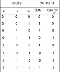
Full Adder
The full adder is responsible for the primary function accomplished by the system. It takes in
three inputs and returns two outputs according to the following equations:
$$Sum=A\oplus B\oplus C_{in}$$
$$C_{out}=A\circ B+C_{in} \circ (A+B)$$
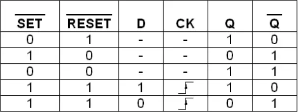
If any one of A, B, or Cin are set to high and the others are set to low, Sum will return high. Cout
stands for carry out, meaning that if at least two of the inputs are true the result will be carried out. When all three inputs are set to high, both outputs will be set to high.
The function of the full adder can be easily determined according to what nodes "Sum" and
"Cout" connect to. As was just mentioned, Cout is only concerned with two or three inputs being
true. However, it can ignore one of the inputs once it has determined that two of the inputs are
already true. This narrows down the number of comparisons that need to be made to three, as
that is the number of input configurations in which two inputs can be high and one can be false.
This is why Cout need not be connected to the rightmost transistor configuration, which opens
when all three inputs are true. Carry Out logic is handled by the three leftmost transistor
configurations. Sum is set to high when one or all three of the inputs are true. What this means is
that Sum can check Cout and set itself to low if Cout is high, unless all three inputs are set to
high. This particular setup is very clever and reduces the number of required transistors when
compared to what would be required to compute Cout and Sum separately.
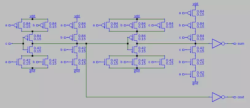
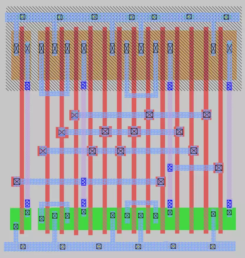
The magic layout of the FA is
harder to match to the Sue layout
especially when compared to the
xor or mux21. Attempting to do
so in words is not worth doing
due to the complexity
The two below images were
compared against the truth table
to verify their functionality. The
top-most of the two images is the
IRSIM result of the provided Sue schematic, while the lower image is of my own VLSI drawing.
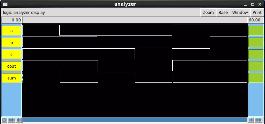
The Sue simulation addresses all input possibilities in terms of the number of true inputs (one,
two, or all three being true). The results of the sue test were successful as expected.
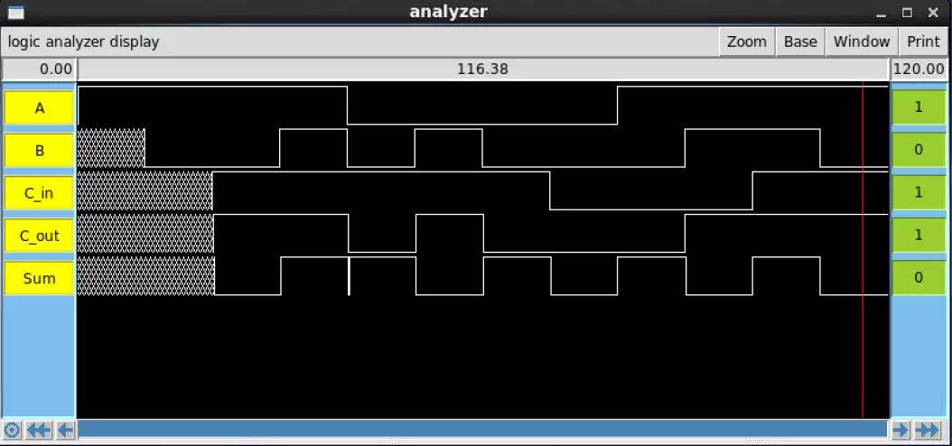
The LVSI Magic implementation passed its IRSIM too, albeit with unnecessary uncertain values
(otherwise known as X values) for the first two cycles. This occurred as a result of the fact that
not all inputs had been set. Thus the first two cycles should be ignored.
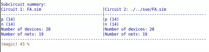
LVS testing of the Full Adder showed the Magic implementation to be identical to the Sue file.
Register
The D-Flip-Flop Register is by far the hardest of the four system elements to both implement and
explain. Put simply, the register will store the value of the Full Adder Sum once its clock input
rises from low to high. This functionality is further complicated by the addition of a nand gate.
However, this will be addressed later in the report. If the clock input into the register is not rising
(changing from low to high), the output Q will remain unchanged regardless of the new input D.
This additional complexity makes an output equation less useful when compared to the
aforementioned elements.
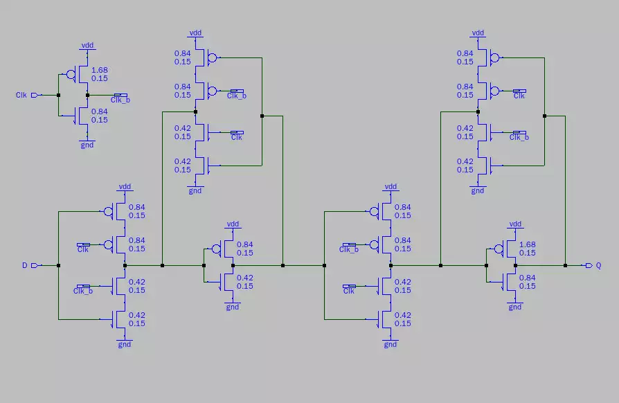
The top left of the schematic lies the clock inverter: the simplest portion of the entire design.
Following the D input from the bottom left of the design is the easiest way to understand how the
register works. If D is set to high but Clk is low, D will not be updated. If D is high and Clk is
high, high is produced at the output of the leftmost transistor structure. The next block of logic is
what is used to store the value of Q, where it will be saved until a rising clock allows for it to be
overwritten by a new input value of D.
There is little that can be done to
describe in words the Magic layout
when compared to the Sue
schematic -- just as with the Full
Adder. One must simply follow the
logic step by step.
The two below images were
compared against the truth table to
verify their functionality. The
top-most of the two images is the
IRSIM result of the provided Sue
schematic, while the lower image is
of my own VLSI drawing.
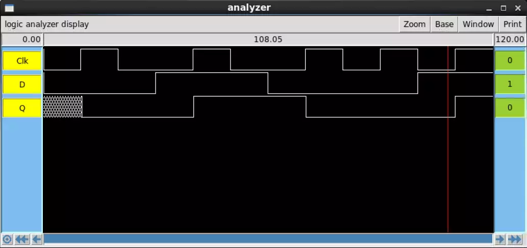
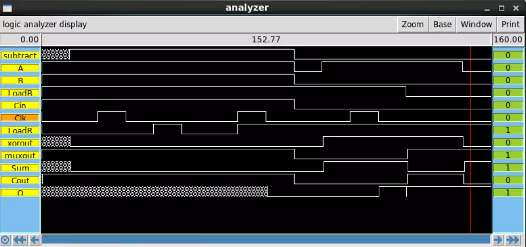
The results of the IRSIM for the Sue and Magic simulations are very simple when compared to
the complexity of the schematic and Magic file. Both simulations work according to the truth
table. LVS testing of the Register showed the Magic implementation to be identical to the Sue file.
1-Bit
All four of the previous components are combined into one to create one bit of the full design.
There are new additions to the circuit however, which are the NAND gate that connects to the
Clk input of the register and the invert which creates the Sel_bar signal. The
NAND equation and truth table are as follows:
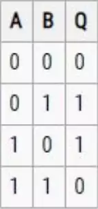
$$Q=\bar{A} \wedge\bar{B}=A\bar{ \wedge}B=\bar{A}\bar{B}=A|B$$
This NAND gate contributes to the function of the register by allowing the
Clk input of the register to be driven to high in accordance with the system
clock and the LoadR (Load Register) signal. The output of the NAND gate
will be low in the case when both the system clock and LoadR signals are
true. Functionality of the new inverter is simply to create the opposite signal
of Sel.
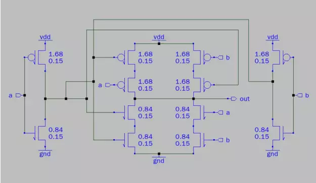
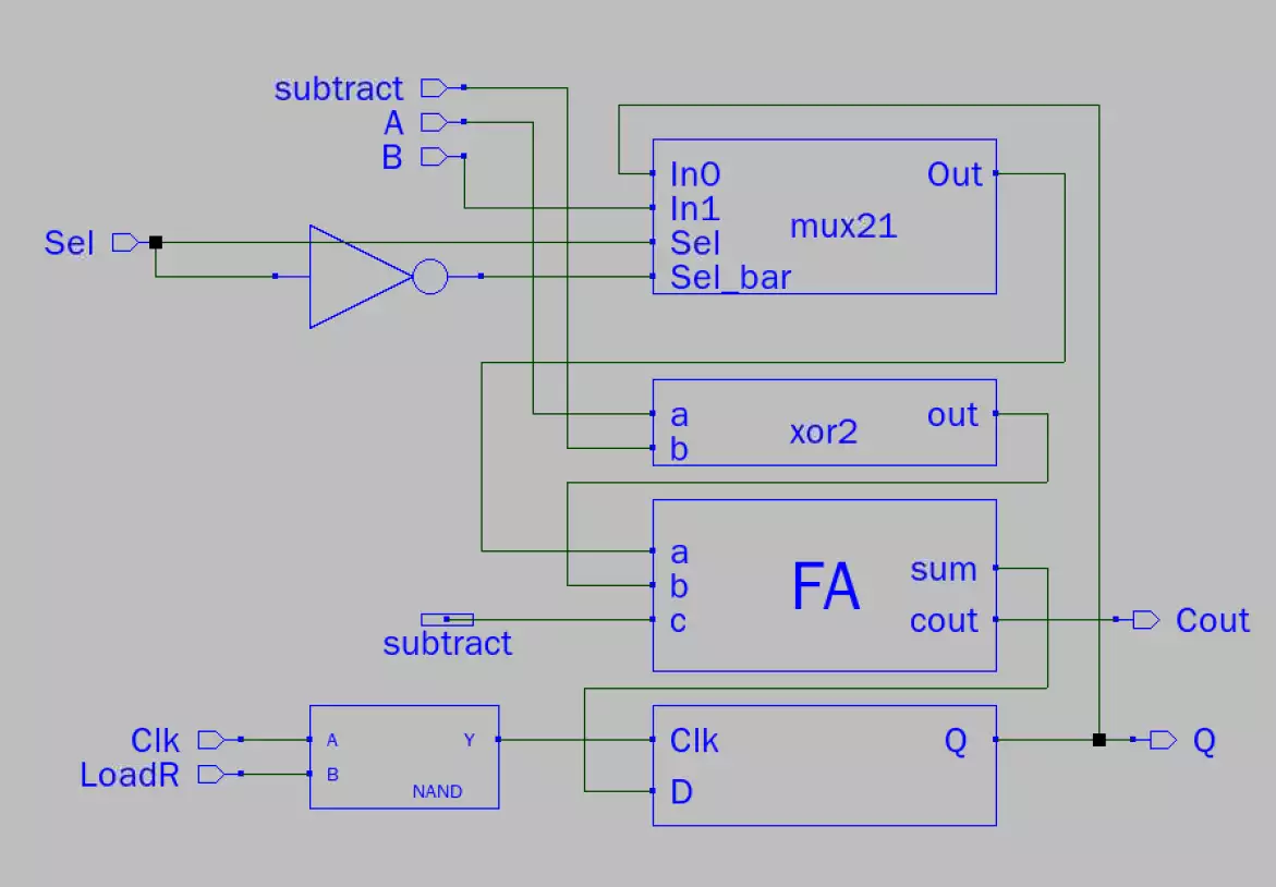
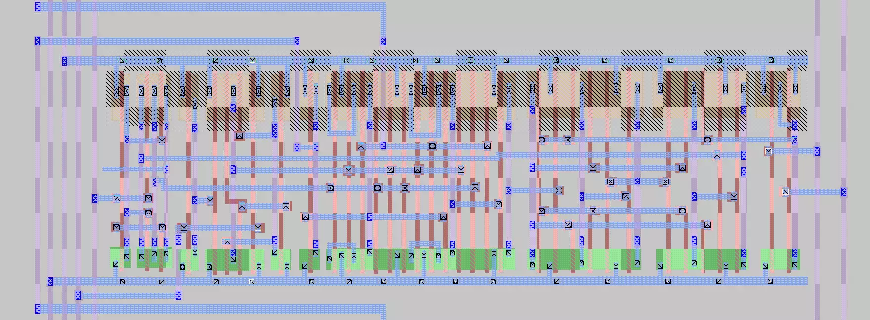
Above is an image of a single bit of the processor in Magic. The complexity of the system has
reached the point where full understanding can only be obtained by referring to previous
sections.
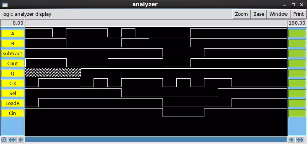
The Sue IRSIM (pictured above) and the Magic IRSIM (pictured below) function identically.
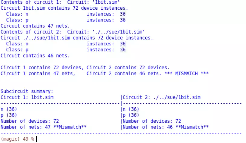
The LVS demonstrates that both the Magic and Sue implementations have identical transistor
counts, but differ in net number by 1. This net difference is caused by the xor Magic
implementation having 1 more net than its respective Sue design. Just as with the xor,
functionality is not influenced by this net mismatch.
Final Design (8-Bit)
Intuitively, the 8-bit schematic is a combination of interconnected single bit designs.
Demonstration that the sue and magic files are identical proves that the system is functioning
properly.
The above image is the final Sue implementation and
uses many name_nets to make the logic easy to
follow. Order of the bits is important when it comes
to the connection of the Full Adders. This is because
the carry out of bit one must go to bit 2, bit 2 's carry
out must go to bit 3, and so on. The order starts with
bit 1 in the top left, numbering down to bit 4 in the
bottom left. Bit 4 connects to bit 5 in the top right,
which finally counts down to 8 in the bottom left.
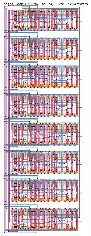
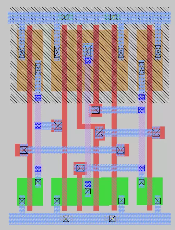
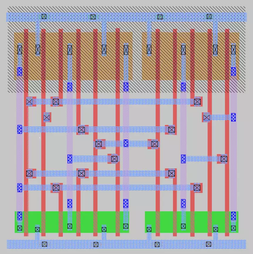
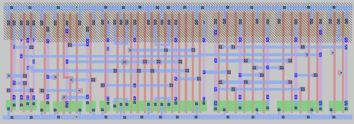
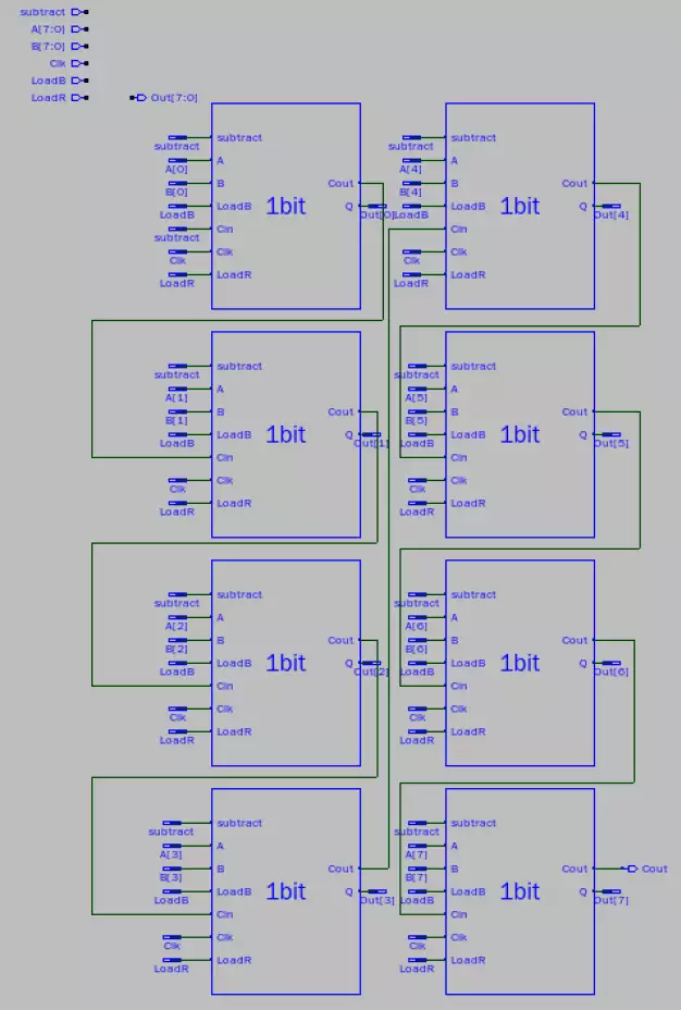
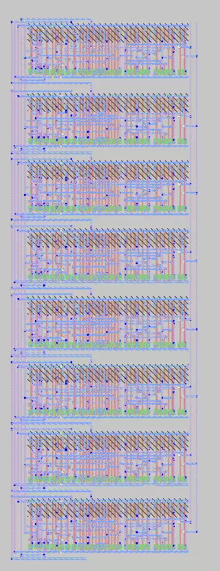
On the right of the page is the final Magic floorplan
of the system. The Magic system is vertically stacked
in terms of bit layout, starting with bit 1 at the top
and ending with bit 8 at the bottom. The system has a
small and efficient design, however it could be
further compressed to save space if necessary. An
additional picture of a single bit of the full eight bit
system is pictured below:
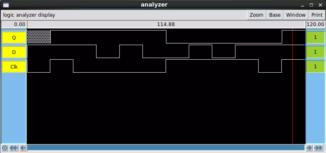
The number of output possibilities becomes massive
due to the exponential nature of the system. In total
there are 768*((28)*(28)*(28)) different combinations of
the vector components of the system. These vectors
are the inputs "A," "B," and the output "Q." The
other input signals further multiply this number by 2
for each signal, resulting in a massive 12288 unique
combinations!
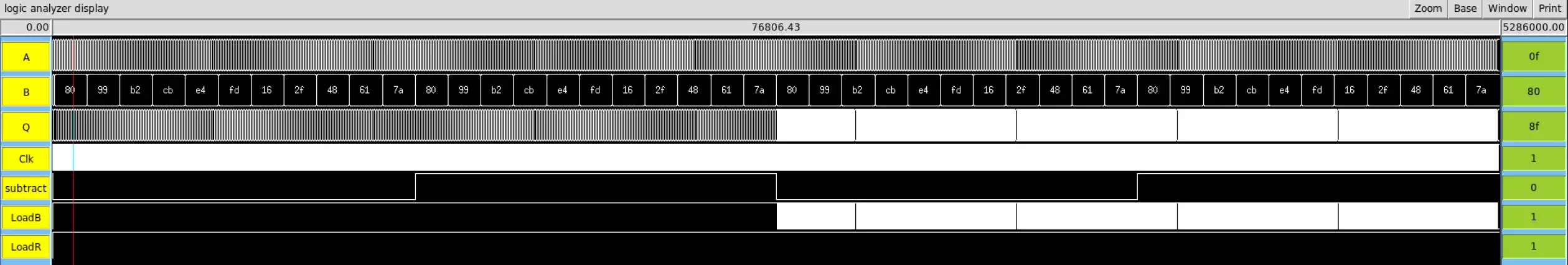
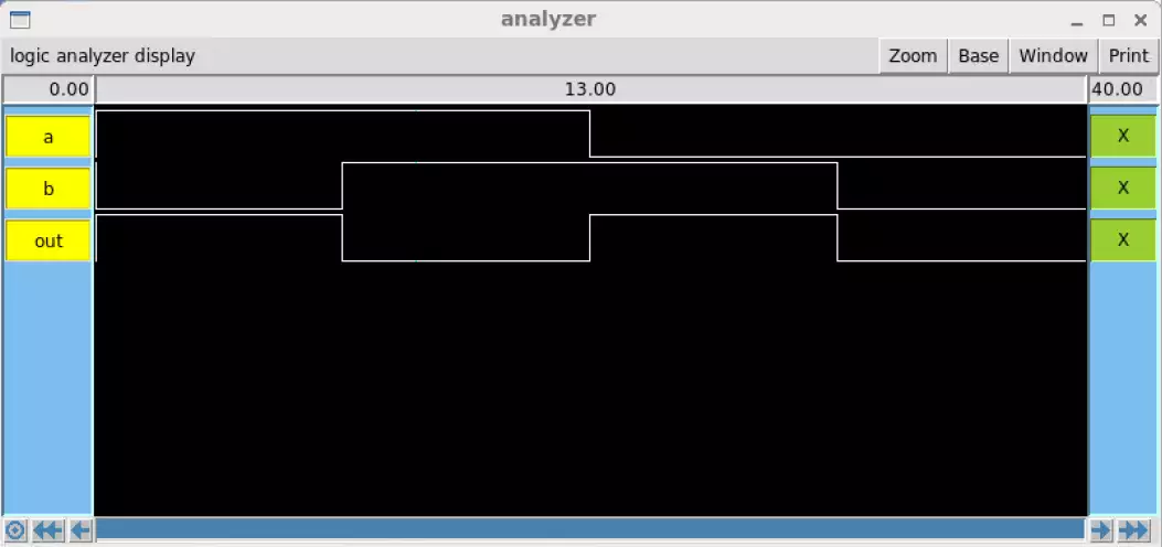
The above image is the output for both the Sue simulation and the Magic simulation. No data can be viewed from this picture due
to its small size relative to the amount of data, but the identical waveforms
demonstrates that they are giving the same output! Below is a closer image of the Magic
floorplan:
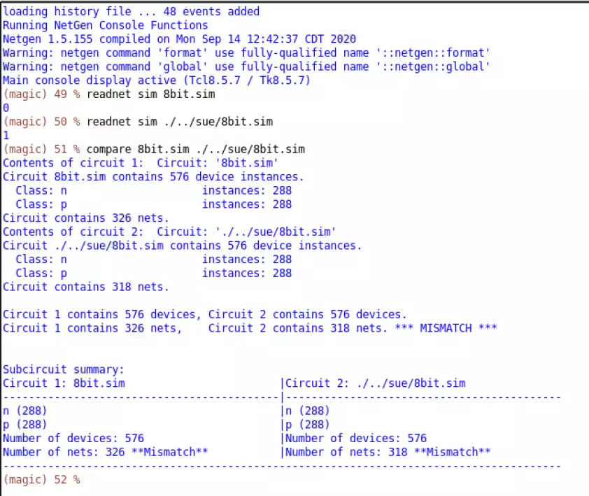
The LVS showcases an identical transistor count, but a net difference just as with the 1bit test.
This difference is due to the net difference of one between the sue xor design and the magic xor
design. This net mismatch has multiplied by eight due to the inclusion of eight xor gates
throughout the entire system. Despite this, the systems work identically!